This project was done in collaboration with my teammates in EGR334 at ASU.
Introduction
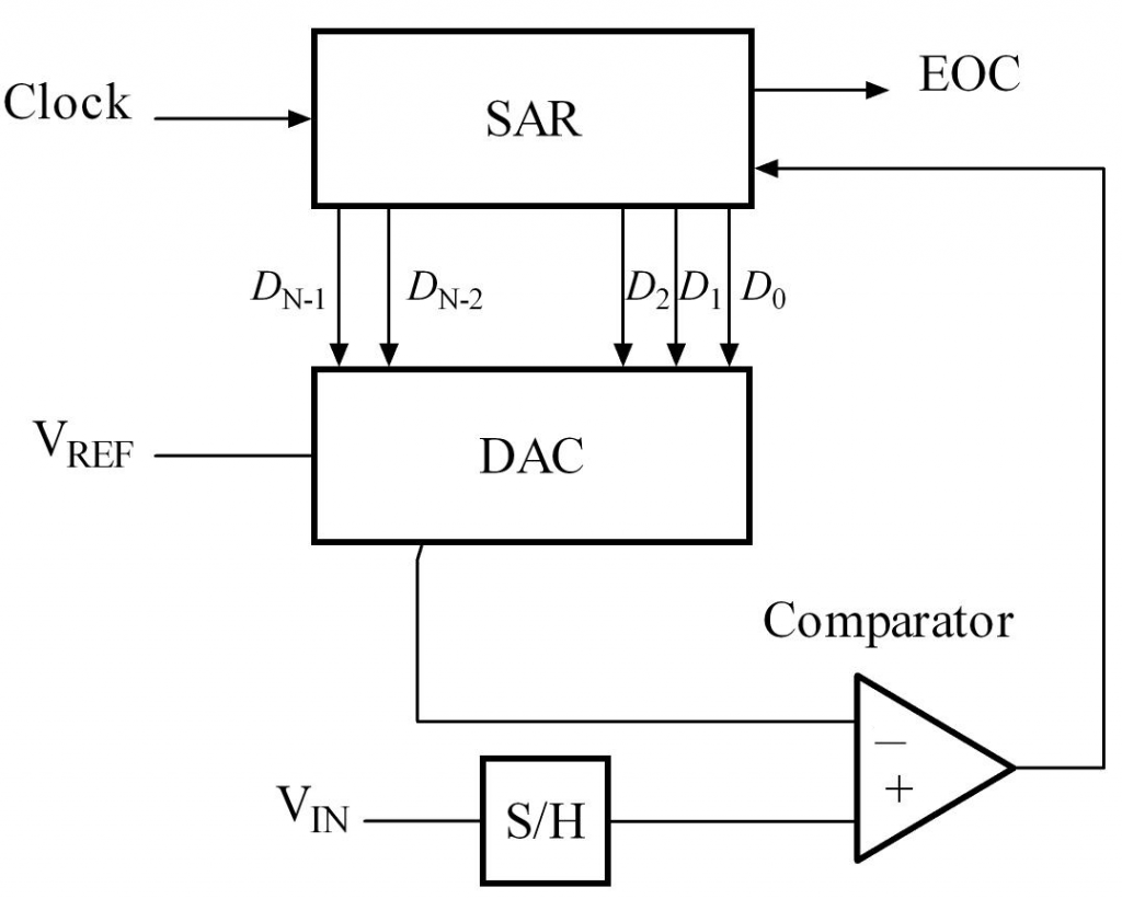
Many analog-digital converters work by having a successive approximation register (SAR) digitally approximate (guess) a voltage, and having an op- amp comparator compare the guessed voltage to the analog input. The output of the comparator tells the SAR whether to increase or decrease it’s guessed voltage. A block diagram for a SAR ADC is shown on the right.
The SAR’s “guess” begins at 0v (binary: 0000). The DAC turns this into an analog voltage (0v), and a comparator compares it to the input voltage (from the sample/hold network; not included in project). The comparator feeds back into the SAR, telling it whether to increase or decrease it’s guessed value (between 0000, and 1111).
For the purposes of this project, the sample/hold network is omitted due to a relatively constant input voltage from a potentiometer. A four-bit ADC will be designed to digitally represent the voltage (between 0 and 5v) as a number between 0 and 16. This four-bit ADC will consist of three primary subcomponents: the successive approximation register (SAR), the digital-analog converter (DAC), and the op-amp comparator.
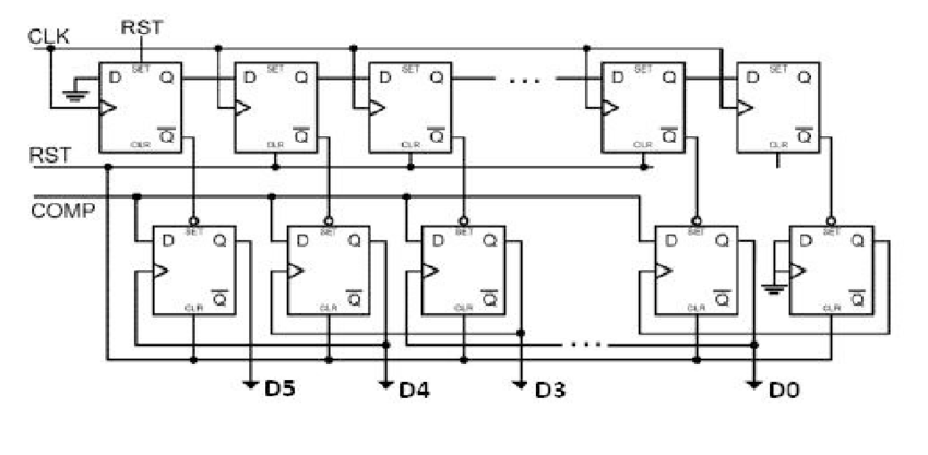
SAR Logic Network
The SAR is initially set to a value wherein the most significant bit (MSB) is set to 1. This mid-range approximation is fed into the digital-to-analog-converter (DAC), which generates a representative voltage that gets compared to Vin. If the DAC voltage is higher than Vin, the SAR will decrement, and if the DAC voltage is lower than Vin, the SAR will increment. When the conversion process is complete, the bits in the SAR are representative of the closest digital approximation to the supplied input voltage at Vin.
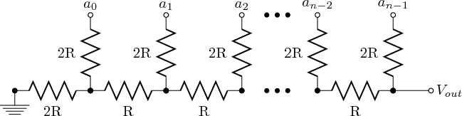
Digital-to-Analog Converter (DAC)
Digital-to-analog conversion is performed using a resistor ladder (also known as an R-2R network, for visually-evident reasons). The idea behind this system is to create an increasing voltage divider between each bit and ground, effectively dividing the voltage by a higher amount when more significant bits are selected. As higher numbers are inputted, the output voltage Vout is increased.
Comparator
The comparator is responsible for comparing the analog output of the DAC and the input signal. Depending on the value, it passes a 1 or 0 to the SAR indicating whether to increment or decrement on the next clock cycle. In this way, the comparator is responsible for getting the output voltage from the DAC to be as close to the input voltage as possible.
Because a comparator is very basic functionality for many op-amps, not much setup is required for this component and it can be used directly with the output of the DAC and the input voltage, provided both are within range of the component.
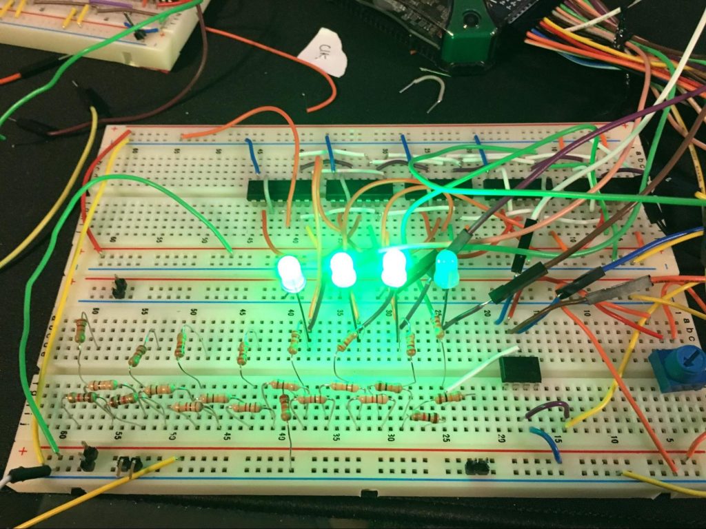
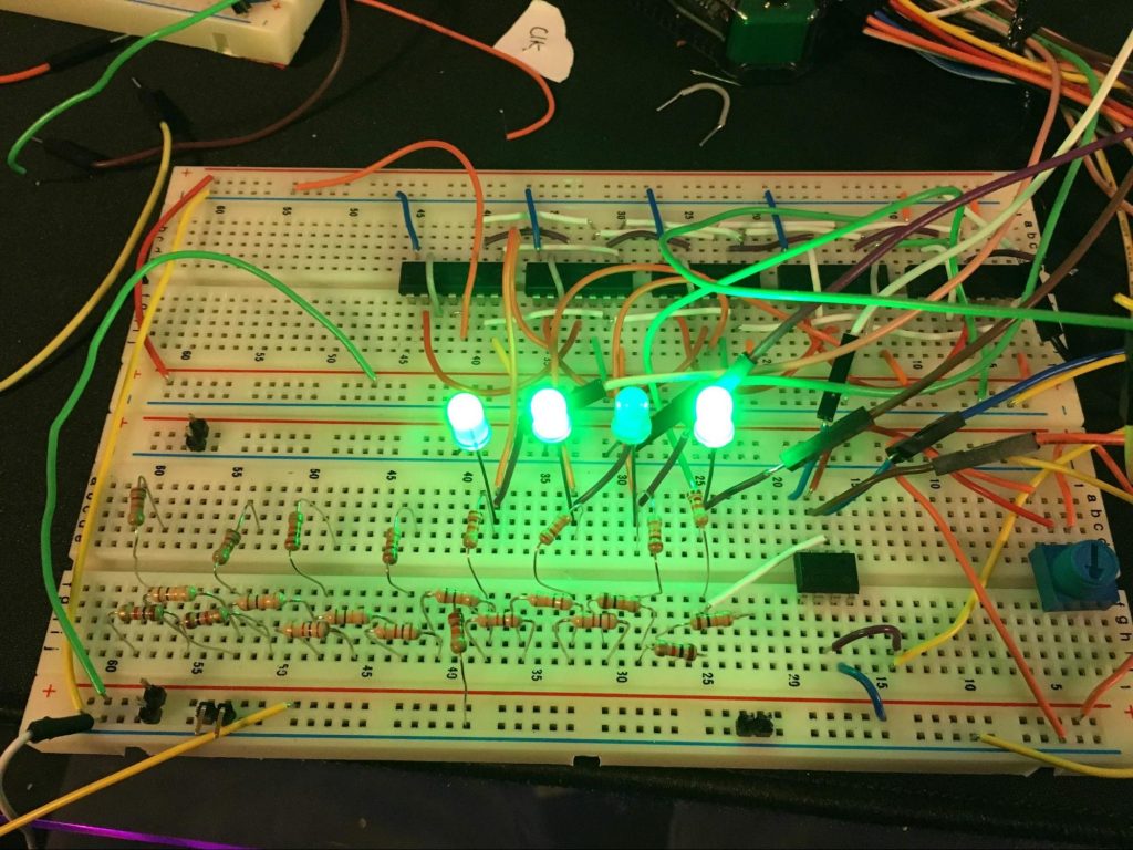
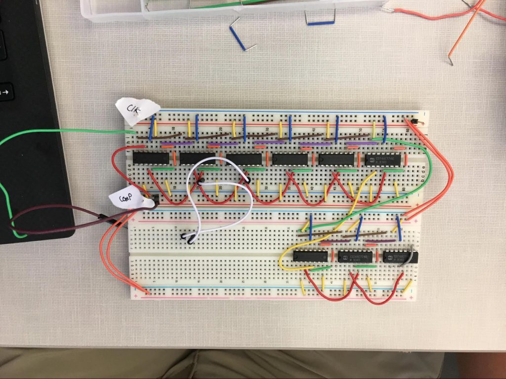
Constructed Circuit
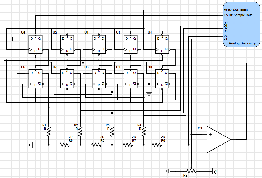
The schematic shown above was constructed using an LM741 op-amp and SN74LS74 D-type flip-flops. A Digilent Analog Discovery 2 was used to provide clock signals for the sample rate and digital logic.
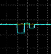
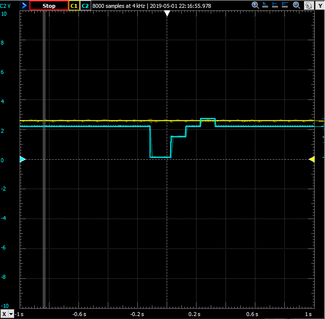
Ideally, the SAR network should begin guessing voltages once the sample rate clock is triggered (rising edge). From there, the SAR should guess several voltages until it finds the voltage corresponding to a binary number that is closest to the input voltage. With the analog discovery connected to the potentiometer on one input, and the output of the DAC to the other, as the potentiometer is turned, the SAR should visibly guess the output voltage.
In the photos below, the MSB and LSB are swapped (so LSB is on the left, and MSB is on the right)
 |
 |
 |
 |
Device build
References
[1] All About Circuits. Successive Approximation ADC [Online]. Available: https://www.allaboutcircuits.com/textbook/digital/chpt-13/successive-approximation-adc/. [Accessed May 1, 2019].
[2] ResearchGate. (2008, Dec.) Successive Approximation Register Schematic [Online]. Available: https://www.researchgate.net/figure/Successive-approximation-register-schematic_fig7_241320822. [Accessed May 1, 2019].
[3] Texas Instruments. (2015, Oct.) LM741 Operational Amplifier [Online]. Available: https://www.ti.com/lit/ds/symlink/lm741.pdf. [Accessed May 1, 2019]
[4] Texas Instruments. (1988, Mar.) Dual D-type Positive Edge Triggered Flip Flops With Preset and Clear [Online]. Available: https://www.ti.com/lit/ds/symlink/sn54s74.pdf. [Accessed May 1, 2019].
[5] Wikipedia. (2019, Mar.) Resistor Ladder [Online]. Available: https://en.wikipedia.org/wiki/Resistor_ladder#/media/File:R2r-ladder.png. [Accessed May 1, 2019]. (I know, I know)
[6] Wikipedia. (2019, Mar.) Successive Approximation ADC [Online]. Available: https://en.wikipedia.org/wiki/Successive_approximation_ADC. [Accessed May 1, 2019]. (I know, I know)