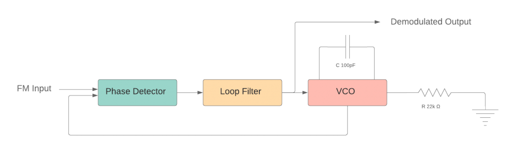
Phase-Locked Loops (PLLs) are widely used in technologies that require motor speed controls, tracking filters, frequency synthesis providing multiple of a reference signal frequency, and frequency shift keying or FSK that decodes for demodulation carrier frequencies. For our project, we will be using a phase-locked loop to demodulate an existing frequency modulated signal. This can be done by allowing the PLL to lock onto the frequency of an input waveform. This is accomplished through the use of a phase detector, a low-pass filter or also known as a loop filter, and a voltage controlled oscillator (VCO). All of which are combined into a negative-feedback system as shown below in figure 1.
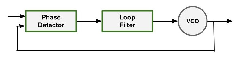
Once the PLL has successfully locked it will produce an output sinusoid that exactly mirrors the input voltage. Do to our application of FM demodulation, the output sinusoid with the same frequency as the input signal isn’t particularly useful. We will instead be using the output from the loop filter as the demodulated signal. This can be summarized:
- The phase detector produces a signal proportional to the phase difference between the output of the
voltage-controlled oscillator and the input waveform. - The loop filter reduces the noise of the signal for the voltage-controlled oscillator.
- The signal then becomes the control signal for the voltage-controlled oscillator.
The voltage controlling the VCO must oscillate with the same frequency as the originally modulated waveform,
and this output can be taken as the FM demodulated output.
Background: Amplitude modulation
Analog information such as sound pressure (an audio wave) can be represented in analog electronics with a voltage. Relatively low frequency signals are considered “baseband” and are very often modulated into high frequency signals for the purpose of effective transmission. A cheap and simple, but relatively ineffective way of modulating a data signal into a high-frequency transmission signal is through amplitude modulation (AM). Amplitude modulation is relatively easy to visualize, as both the carrier and the data wave are clearly visible in Figure 2.
The data can be viewed in a more complex way by applying a Fast Fourier Transform (FFT) to the data, and graphing this FFT over time in what’s known as a spectrogram, shown in Figure 3. Note the constant, red signal visible at 1MHz: the carrier frequency. The data signals, once modulated into the AM signal, appear in the frequencies directly above and below the carrier frequency, known as “side bands.” An additional spectrogram for a different AM 200kHz data signal is shown in Figure 4.
 |
 |
 |
There’s nothing particularly remarkable about the spectrogram for this AM signal, and while we’ve complexified our illustration of the waveform, AM lags behind in complexity. Note how the frequency appears in the spectrogram: constant through time. The waveform contains the baseband signal in the amplitude of the side bands.
Background: Frequency Modulation
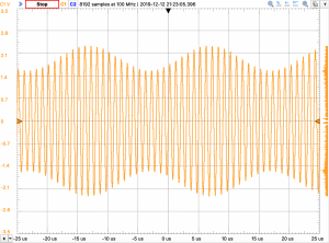
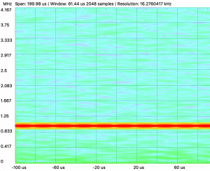
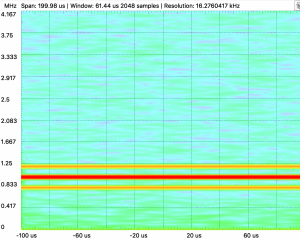
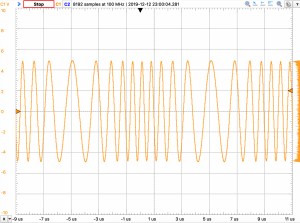
Frequency modulation is traditionally more difficult to visualize. You can crank the modulation index up to 50% and try to “imagine” what the frequencies would look like after seeing the time domain (Figure 5), but a spectrogram of an FM waveform is much more clear.
 |
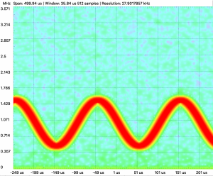 |
Notice how we’re able to understand a lot more about the FM waveform through the spectrogram. In amplitude modulation, data is encoded in the side bands of the transmission, while in FM, we can see that the frequency of the waveform itself encodes the data by oscillating according to the modulation index: 50% illustrated. This is a much more reliable approach, however costing complexity. Because of the intricate nature of an FM signal, more care is required in the demodulation process.
The scope of this project is centered around demodulating an already-modulated FM signal, so the creation of the FM signal will not be discussed. Nevertheless, a firm understanding of the mechanics of frequency modulation is essential to designing a demodulator.
FM Demodulation
There are several approaches to demodulating an FM signal, but this project focuses on using hardware known as a Phase-Locked Loop (PLL). The PLL is common in many household electronics, and typically appears in FM radio receivers. It consists of a phase detector, a loop filter, and a voltage controlled oscillator.
The input to the PLL is, of course, the FM modulated signal. The output is also the FM modulated signal, which is relatively inconsequential for the purposes of demodulation.
VCO: The VCO is an oscillator that should be configured to naturally oscillate at the carrier frequency of the incoming FM wave. By changing the input voltage in the VCO, the output frequency is changed slightly.
Phase Detector: The phase detector takes two inputs: the FM signal and the output from the VCO. The premise behind the phase detector is that a signal is generated proportional to the phase difference of the two incoming waves. The output of the phase detector is filtered, and then applied directly to the VCO.
Loop Filter: Responsible for filtering the output of the phase detector so it’s suitable for input into the VCO. The output of this filter is the demodulated signal.
The premise behind the PLL is to take the incoming FM signal and the signal generated by the VCO, and adjust the VCO’s output so it exactly matches the incoming FM waveform. As the VCO’s output is exactly the same as the FM signal, the input to the VCO must be the modulated data signal.
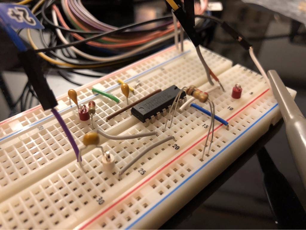
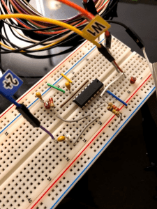
Physical Setup
Hardware Requirements
- CD74HC4046A Phase-Locked Loop with VCO and Lock Detector.
- Resistors (22k, 100k)
- Capacitors (100pF, 1000pF)
- Piezoelectric transducer to act as a speaker to demonstrate demodulated output (optional)
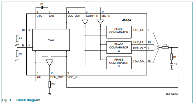
Block Diagram of PLL Components
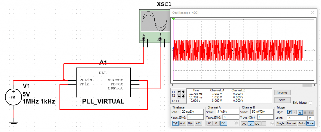
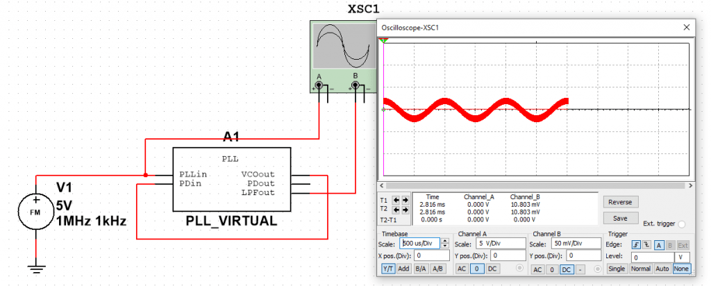
Multisim PLL Circuit Simulation
Component Configuration
The datasheet for the PLL provides a general connection strategy. The device provides the choice between three different phase comparators. For the purposes of this project, Phase Comparator 1 will be used. Components R3, R4, and C2 are part of the low pass filter, which will be discussed shortly. The output of the filter is fed to VCO_IN. The VCO is configured using C1, R1, and R2 as specified in the datasheet.
Selection of R1 and C1
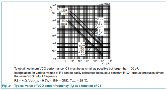
The datasheet provides some insight as to the choice of R1 and C1 in order to choose the VCO’s center frequency. The datasheet indicates that for maximum stability, C1 can be selected to be 100pF. To achieve the VCO center frequency of 1MHz, the resistor value R1 is interpolated to find the correct value. This interpolation process is described more in depth.
As shown in Figure 15, the datasheet indicates that the frequency increase is relatively linear. Figure 14 allows us to interpolate a resistor value R1 that centers the VCO frequency at 1MHz.
With the center frequency at 10 MHz, R1 is found to be 3k. With the center frequency at 1.1 kHz, R1 is found to be 300k. Using interpolation, for a frequency of 1MHz, resistor 1 should be selected to be approximately 15k. Due to material availability, a 22k resistor will be used.
The datasheet also describes the functionality of R2. R2 allows for frequency offset to be applied to the FM demodulation. Since the modulated signal in this project is a baseband signal, no frequency offset will be applied. With no frequency offset, R2 is selected to be infinite impedance, and is left open. Finally, Rs is selected to be 100k to apply load to the DEM_OUT pin per the datasheet.
Selection of Low Pass Filter
The datasheet also provides significant information on Low Pass Filter selection.
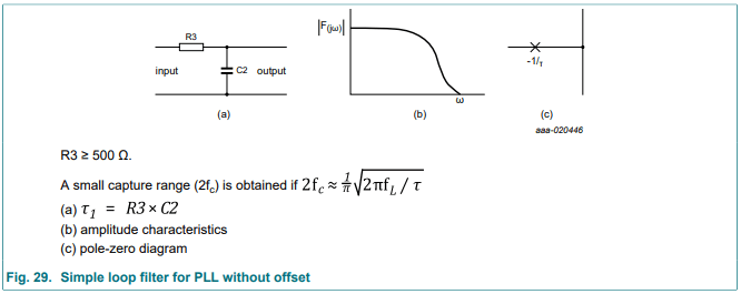
The low pass filter is responsible for filtering the input into the VCO, which should look identical to the original modulated input frequency. In this project, baseband signals will be modulated into the carrier frequency, and there can be reasonable confidence that the modulated signal will never exceed 10kHz. As such, a capture frequency, 2fC of 10kHz will be selected for the low pass filter.
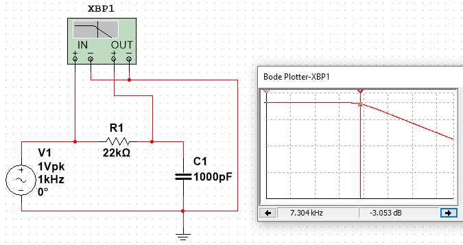
The datasheet guides the math on resistor and capacitor selection. Due to component availability, a 1000pF capacitor will be used. The capture frequency 2fC will be set as 10kHz, and the lock frequency is determined by the modulation index of the input signal. For this project, a modulation index of 20% will be used. The lock frequency is also determined by the datasheet, and is set at 5000 Hz. The time constant tau can be calculated using their given equation, and used to select the resistor.
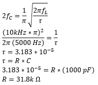
Due to component availability, the capture frequency of the low pass filter will be increased slightly so a 22k resistor can be used. The low pass filter, using a 1000pF capacitor and a 22k resistor, was simulated in multisim to ensure the correct frequencies are removed.
Low Pass Filter Multisim Simulation
The final design of the circuit follows the block diagram specified in the datasheet. Passive components are added to configure the device. The center frequency, fC is set at 1MHz. The lock frequency, 2fL is set to the modulation index, 20% of the carrier frequency, or 10kHz. With all components of the device selected, the PLL can be tested with an FM waveform from the Analog Discovery 2.
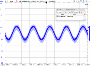
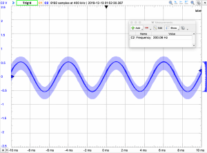
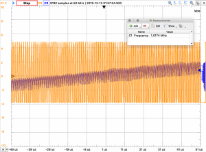
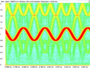
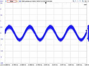
Device Testing
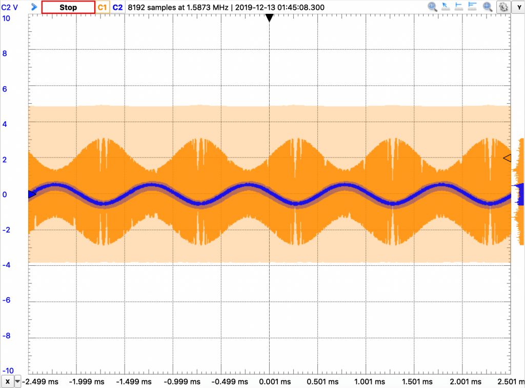
The device is run with several baseband data frequencies modulated into a 1MHz carrier wave. As long as the data signal is low frequency enough to pass through the low pass filter, the device is successfully able to demodulate various FM signals. Several demodulated outputs are shown below:
 |
 |
Some More Images
 |
 |
 |
 |